Source: pv tech

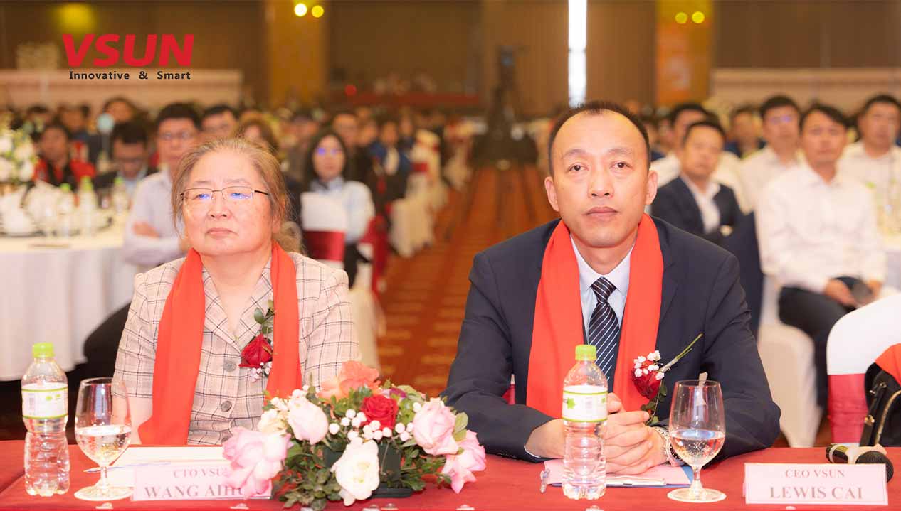
Dr. Wang, a highly-respected figure in the field of high-efficiency solar cell technology, made recent headlines with her appointment as Chief Technology Officer at VSUN. Her decision to re-engage with the industry has generated speculation over the influence and change she may bring to both the company and the sector at large. PV Tech sat down with her in an exclusive interview to discuss these and other related topics.
By way of background and perspective, in 2023 the husband-and-wife team of PV scientists Jianhua Zhao and Aihua Wang were joint recipients of the prestigious Queen Elizabeth award for engineering, described by some as the engineering sector’s Nobel Prize, their contribution to the research into and implementation of PERC solar cell technology being key to the PV industry and highly impactful on the field of high-efficiency cell technology.
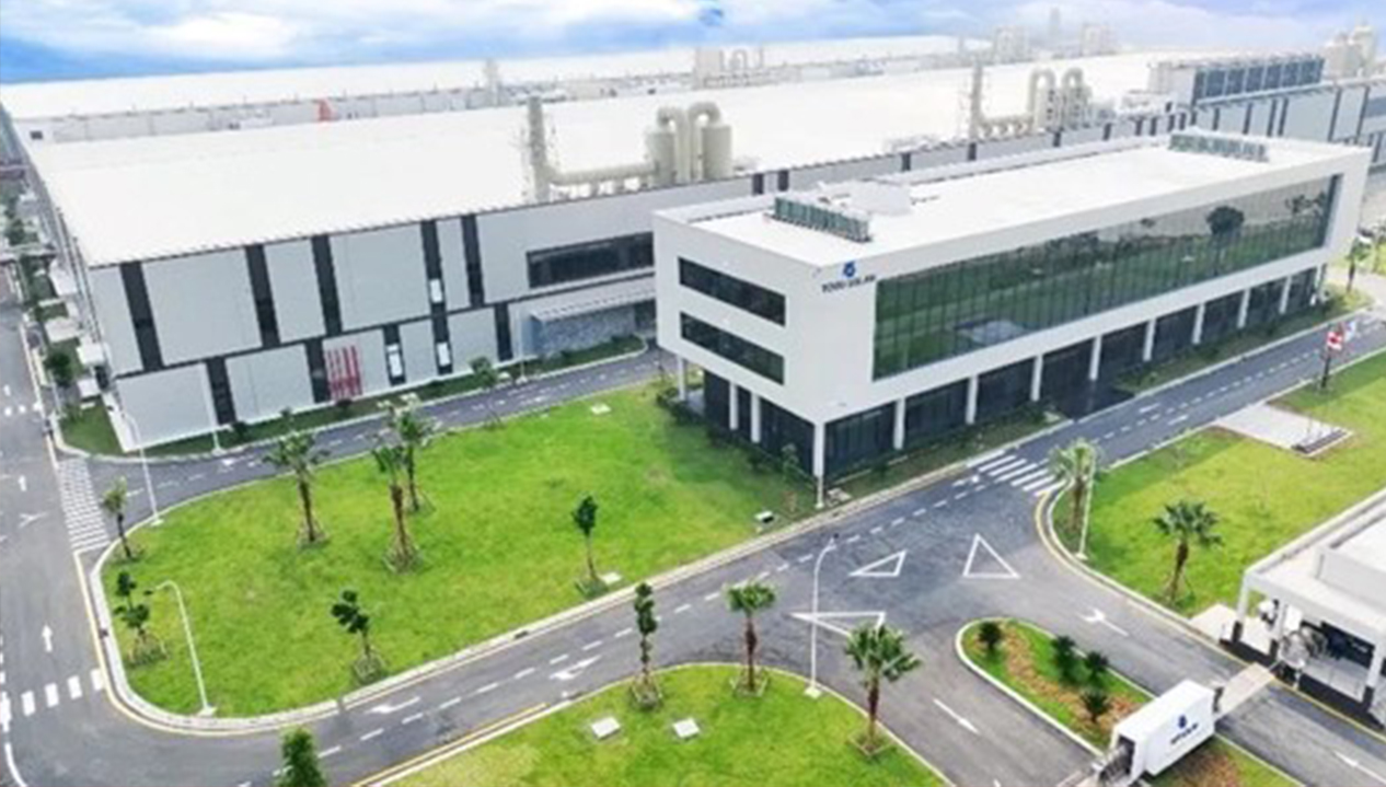
VSUN is a provider of solar panel solutions. Headquartered in Tokyo, Japan, and with financial backing from Fuji Solar, the company offers reliable, efficient products and technology on a global scale. VSUN currently has 4GW of module production capacity in Vietnam, with a further 4GW capacity for TOPCon cells and a planned 4GW capacity for silicon wafers. Integrating Japanese quality management systems and consolidating PV resources, the company aims to establish a vertically integrated global supply chain.
Dr. Aihua Wang: Firstly, I was genuinely moved by CEO Lewis Cai’s invitation. Secondly, as a company, VSUN is on an impressive growth trajectory, having strategically positioned itself within mainstream cell technologies. Although it may not be as large as some of the major domestic players, the company has its unique advantages. These include experienced Japanese-style management, a solid and reliable team and robust overseas sales networks. The company’s products are currently exported to over 40 countries and regions.
What’s particularly impressive is its growing market share in the United States and Europe. I see great potential in VSUN. The company has established production lines in Vietnam and is expanding its capabilities in cell and silicon wafer production, creating an extensive industrial chain. Another key factor is VSUN’s high brand recognition in international markets, which I believe is crucial for global success.
AW: The company currently has 4GW of production capacity for modules and the same for TOPCon cells in Vietnam, with Phase II of the expansion of cell capacity underway, given the importance of establishing our presence in the upstream supply chain.
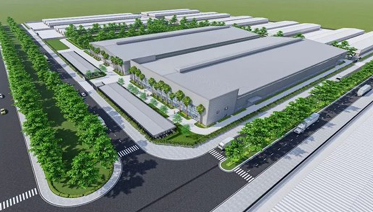
Our silicon wafer factory in Southeast Asia is also under construction, expected to be operational during the second quarter of this year with a planned capacity of 4GW and work is also underway on domestic production capacity in the United States. The first phase includes 2GW of capacity for both cells and modules with factories due to enter operations during the fourth quarter of 2024 and 2025 respectively.
AW: Beyond variations in substrate materials, the primary direction for cell technology development lies in addressing surface passivation issues, with a clear trend toward the evolution from non-passivated to partially passivated contacts. For instance, with TOPCon cells, the backside electrode achieves passivated contact, progressing to HJT which employs full passivation contact, meaning both sides feature passivated contacts.
There are also challenges related to the improvement of stability and efficiency. In terms of efficiency, transitioning from the laboratory to mass production involves different considerations. Mass production necessitates that technical personnel are well-versed in the processes, maintenance of equipment is upheld and the production line undergoes extensive tuning and optimization. VSUN has a solid foundation, and the company’s production lines in Vietnam are performing extremely well.
AW: VSUN’s focus right now is on perfecting our TOPCon technology and gradually expanding our production capacity. We’re also developing other technologies like heterojunction to cater to niche product demands. Looking ahead, I believe that perovskite layering is a promising direction for future advancement, although it remains a technology ‘on the horizon’.

AW: The evolution of mass production cell technology is a process of gradual refinement, with each of the three main technological paths having distinct features and suitable applications. TOPCon cells, for instance, can be developed from existing PERC lines, allowing for the continued use of current equipment. In contrast, HJT requires a new production setup, but benefits from fewer steps and lower processing temperatures.
IBC technology, along with its variations, places both electrodes on the backside, removing the need for front metal grids and thus avoiding shading. This not only boosts efficiency but also offers an aesthetically pleasing appearance. At the moment, I see these three technologies as both competing with and complementing each other.
AW: P-type silicon wafers are known for their simpler manufacturing processes and lower costs, whereas n-type wafers have a longer lifespan and the potential for higher efficiencies, though their production is comparatively more complex. This complexity primarily stems from the differing segregation coefficients of phosphorus and boron in silicon, which introduce a number of challenges in the ingot pulling process.
Initially, the photovoltaic sector relied on the predominantly p-type cells borrowed from space technology applications. However, with the progression in monocrystalline rod pulling equipment and methodologies, n-type silicon wafer costs have also been effectively managed. N-type wafers, in comparison to their p-type counterparts, are better suited for the creation of high-efficiency cells.
Currently, the leading cell technologies based on n-type monocrystalline silicon include HJT, TOPCon and IBC, as well as their integrative and derivative variants like HBC (HJT-IBC) and TBC (TOPCon-IBC). There’s ongoing research into enhanced TOPCon cells that incorporate poly fingers or a complete poly surface on the front, facilitating passivation contact on the front of the TOPCon cell.
The silicon-based solar energy and wide-bandgap semiconductor group at the Ningbo Institute of Materials Technology and Engineering under the Chinese Academy of Sciences has proposed a dual-function polysilicon layer structure utilizing innovative nitrogen-doped polysilicon. This nitrogen-doped polysilicon not only delivers exceptional passivation capabilities but also efficiently extracts charge carriers.
It’s vital for us to undertake our own investigative and developmental work, utilising these advantages to enhance the performance of current cells. Moreover, nitrogen atoms can effectively modulate the optical bandgap of polysilicon and the energy band configuration of TOPCon, enhancing both optical and electrical passivation effects. This research provides significant guidance for the architectural design of high-efficiency TOPCon cells, particularly for designs involving bifacial and full-back contacts, and paves the way for the commercial deployment of novel polysilicon technologies.
AW: N-type technologies, such as TOPCon production lines, demand more from both personnel and equipment compared to their p-type counterparts. This encompasses issues of compatibility with the equipment and poses greater challenges in ensuring product stability, uniformity and consistency.
Prior to the adoption of TOPCon, the complexity of the processes, the control of production lines and the requirement for technical personnel were somewhat easier to manage. Currently, with the increased complexity of processes, the importance of personnel training cannot be overstated. It’s imperative for technical staff to receive comprehensive training. Essentially, successful mass production hinges on seamless coordination among various factors, including process optimization and equipment integration.
The key challenge lies in how to effectively link together multiple complex elements to both enhance efficiency and reduce costs. Moreover, establishing a highly stable baseline process is crucial for enabling further improvements and innovations. On a stable process foundation, it’s much simpler for engineers and technical staff to test new ideas and implement enhancements.
While PERC cells have amassed data spanning over a decade, n-type technologies are relatively new on the scene. It’s therefore vital to not only assess compatibility with production, but also to evaluate real-world performance, which can then be used to inform adjustments and refinements on the production line. Additionally, with the continual emergence of new processes and equipment, it’s important to stay agile, updating technologies and processes in a timely manner to keep in step with the rapid pace of industry evolution.

AW: Thanks to significant advancements in efficiency and process technologies, the rate of progress has certainly surpassed what I had initially imagined. Before 1985, the industry debated whether a 20% efficiency rate was the ceiling for silicon cells. This notion was shattered around 1989 when efficiencies reached 22%, and we’ve seen continual increases since, now surpassing 26%.
I am seeing that the industry’s pace of development has significantly accelerated beyond previous eras. For instance, in R&D, there was once a less pressing urgency, but now the cycle of technological innovation is so swift that today’s research outcomes may be applied in production almost immediately. The industry has seen an enormous increase in investment and scale and, as a result of such explosive growth, collaborative endeavours to instigate change have become relatively easier to achieve than previously.
That said, I believe there’s a need for the industry to momentarily decelerate and escape the cycle of volatile growth, since the pattern of fluctuating between the spirals of booms and surpluses may not be entirely conducive to the sector’s long-term, stable expansion and striking a balance to achieve steady and sustainable progress presents an unavoidable challenge that we must address.
AW: The theoretical efficiency of solar cells is a matter for debate, contingent upon the methodologies, assumptions made and the entity conducting the tests or calculations.
Regarding the future ceiling for crystalline silicon cell efficiency, it’s challenging to pin down a specific forecast to trust. Nonetheless, achieving practical efficiencies in the realm of 28% to 29% would signify a significant plateau, particularly if such levels of efficiency could be realized in mass production. That would mark an exceptionally high standard.
AW: I’ve seen announcements from some companies about the mass production and deployment of perovskite modules. Should perovskite or perovskite-tandem cells overcome the hurdles of durability and reliability, I’d consider them to be an exciting avant-garde technology. It’s imperative to keep a close eye on progress within this area and to commence research and development initiatives in earnest. At present, my familiarity with the mass production and application scenarios for perovskites is somewhat limited and needs further investigation.
By:PV TECH

 Email
Email
 WeChat
 LinkedIn
 Facebook
 Copy link